Speakers
INVITED SPEAKERS: | |
|
Prof. Ray DagastineDepartment of Chemical & Biomolecular Engineering and the Particulate Fluids Processing Centre, The University of Melbourne | Atomic Force Microscopy: Routine applications to complex methods for materials characterisationAtomic Force Microscopy (AFM), invented by the same group that received the Nobel Prize for the invention of the scanning tunnelling microscope, was originally developed as a tool to obtain 3-D topography information on the nano-scale for insulating surfaces. Since its invention thirty years ago, the number of application and uses of AFM has enabled an explosion in the amount of research focused on the visualization of materials at the nano-scale. The extension of the use of AFM to imaging under liquid, atomic scale resolution imaging, conductive AFM, nano-mechanical property mapping and measurement and force spectroscopy methods have driven the uptake and evolution of these methods in a range of fields around material science, soft matter and self assembled systems, polymer physics, biology focusing on biomolecules and living cells, energy materials, semiconductor processing, 2D materials and manymore. Many have expected AFM measurements to become as routine as using a toaster, and this talk will give an overview of the types of capabilities that are often routine in the lab with some of the possible pitfalls for users in analysis. In addition, many applications that use AFM are still more attune to playing a violin, where atomic resolution imaging, some biological applications, sophisticated nano-mechanical methods and a force spectroscopy methods often vary from routine measurements to quite advanced techniques that can require a great deal of expertise. This talk will highlight a number of these methods, some with more detail based on specific research examples in measuring cell stiffness, material property mapping of complex surfaces, compression of micro-capsules, single molecule unfolding, and force spectroscopy between drops and bubbles. Bio: Professor Ray Dagastine is the initiative chair of the Materials Research Hallmark Initiative at The University of Melbourne and is the academic leader of a the Materials Characterisation and Fabrication Platform. His research interests are in the area of particulate and droplet interfacial phenomena, emulsion stability and deformable surfaces. He is a leading researcher in developing experimental methods and theoretical analytical tools to study interaction forces between deformable liquid-liquid interfaces using both optical techniques and atomic force microscopy. He also has research interests in structure in complex fluids, non-equilibrium surface forces, and protein interactions and nanomechanical properties of capsules and micro-particles. |
|
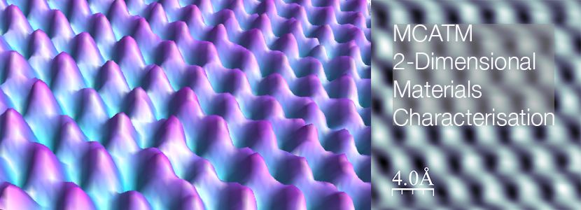
Dr. Lauren HydeMaterials Characterisation and Fabrication Platform, The University of Melbourne | 2D materials characterisation capabilities at The University of MelbourneThe Materials Characterisation and Fabrication Platform (MCFP) supports materials research through advanced instrumentation, analysis and characterisation. The platform facilitates access to a range of complementary technologies, focusing on atomic force microscopy, super-resolution microscopy, nanofabrication, mass cytometry and X-ray diffractionComprised of 4 nodes; Nanomaterials Characterisation, Advanced Fluorescence Imaging, X-Ray Diffraction and Nanofabricaiton, our team of dedicated technical specialists can provide training, advice on experiment design, as well as fee-for service measurements and analysis. The MCFP welcomes all users across the scientific community, from universities and research institutes to industry. This talk will highlight the many MCFP operated materials characterisation capabilities available to researchers, with a particular emphasis on how they can be applied to characterise 2D materials. Bio: Dr.Lauren Hyde is the Platform Manager of the Materials Characterisation and Fabrication Platform at the University of Melbourne. Lauren has a background in nanotechnology and a PhD in biomaterials science. Previously, she has managed the Vibrational Spectroscopy facility at the University of Sydney and was a beamline scientist on the infrared microspectroscopy beamline at the Australian Synchrotron. Lauren has joined the MCFP team as the platform manager in 2013. She has experience with many surface topography and chemistry preparation methods as well as surface analysis experience including infrared and Raman microscopy, atomic force microscopy (AFM) and scanning electron microscopy (SEM). |
|
Dr. Scott FindlaySchool of Physics & Astronomy, Monash University
A/Prof. Matthew WeylandDepartment of Materials Science & Engineering and Monash Centre for Electron Microscopy, Monash University | Atomic-resolution imaging of atomically thin materials via transmission electron microscopyTransmission electron microscopy (TEM), in both conventional and scanning modes and making use of aberration-corrected optics, can image the structure of atomically-thin materials with atomic resolution. This enables direct, atomic-level visualization of defect and dislocation structures, stable sites for individual atoms and nanoclusters suspended on the atomically-thin material’s surface, charge redistribution around dopants, and measurement of strain. It can also, via spectroscopic techniques, offer local information on the chemistry, electrical properties and bonding of the specimen. However, atomically-thin materials are often beam-sensitive, meaning that their structure may be modified or damaged by the probing electron beam, and care is needed to distinguish intrinsic structures from those induced by beam damage. This talk will present the capabilities of advanced TEM for exploring the structure of atomically-thin materials. It will overview some of the main TEM imaging modes applied to imaging atomically thin materials and the information they contain, using examples from the recent literature. It will also cover practical aspects of preparing specimens for TEM imaging and the appropriate experimental conditions for imaging these often beam-sensitive specimens. Bios: Dr Scott Findlay completed his PhD in Physics at the University of Melbourne in 2005. He was a Japan Society for the Promotion of Science Postdoctoral Fellow at the Institute for Engineering Innovation at the University of Tokyo from 2008 to 2010, and a QEII Fellow in the School of Physics and Astronomy at Monash University from 2011 to 2015. His research centres upon using theory and numerical modelling to develop new approaches to imaging and quantitative analysis in scanning transmission electron microscopy. A/Prof. Matthew Weyland, manages Australia’s first aberration corrected TEM, the FEI Titan3, and drives research using this instrument. Matthew’s research centres on the development of electron microscopy, and its application to materials problems. He has published in nearly all areas of materials science, from polymers to metals, magnetic materials to catalysts, and electronic materials to corrosion. In recent years his publications have mainly been on the atomic structure of light alloys (Al, Mg etc), semiconductor heterostructures and functional nanoparticles. |
|
A/Prof. Laure BourgeoisDepartment of Materials Science & Engineering and Monash Centre for Electron Microscopy, Monash University | Transmission electron microscopy of curved graphitic surfacesLayered crystal structures can display an astonishing variety of topologies, from spheres, tubes and cones to the more exotic negatively curved surfaces. The best-known family of curved surfaces is carbon, with “flat” graphite able to curve into an atomically thin sphere (C60), tube (carbon nanotube), cone or saddle. This talk will present an overview of past and present work on the characterisation of such structures by transmission electron microscopy. This technique has been an important tool in the structural determination of curved nanoscale materials. We will focus on carbon and boron nitride, but will also briefly introduce lesser known “curved crystals”. Bio: A/Prof. Laure Bourgeois’s main research interest lies in the determination of atomic-scale structure in inorganic materials, with emphasis on nanoscale crystals, crystalline defects and aperiodic phases (incommensurate crystalline phases, quasicrystals, but also curved graphitic structures). Structure is a fundamental starting point to the science and engineering of materials and minerals, and this is the main motivation behind Laure’s work. More specifically, structural information has been used to gain an understanding of the mechanisms of solid-state nucleation and growth in a variety of systems, with the current focus being on light alloys. To achieve this, Laure uses a variety of techniques available in the great versatile tool that is transmission electron microscopy (TEM), in particular atomic resolution imaging techniques such as high-angle annular dark field (HAADF) scanning (S)TEM and high-resolution TEM in conventional and aberration-corrected transmission electron microscopes. |
|
Prof. Michael JamesAustralian Synchrotron | A landmark national research facility shining light across a diverse scientific landscapeThe Australian Synchrotron is one of Australia’s premier research facilities and, at about $300 million, represents one of the biggest single investments in scientific excellence in the nation’s history. Operated by the Australian Nuclear Science and Technology Organisation, the Australian Synchrotron produces intense beams of X-ray and infrared light at its ten experimental endstations, providing unique research capabilities. The Australian Synchrotron is not only an experimental facility, staffed by ~135 scientists, engineers, technicians, and support staff. At its heart are two highly tuned electron accelerators: a 100 million volt (MeV) linear accelerator that sets packets of electrons moving at relativistic speeds just under the speed of light, before injecting then into the 3 billion volt (3 GeV) booster synchrotron that increases their mass by a factor of ~60. As these high-energy packets of electrons interact with specialised magnetic devices that steer and focus the electron beam around the synchrotron storage ring they generate intense beams of synchrotron light that are used for a huge range of research applications. Bio: Michael has a BSc from the University of Sydney and a PhD in inorganic chemistry from the University of Cambridge, UK. Prior to joining the Australian Synchrotron as Head of Science in January 2013, he was a senior principal research scientist at ANSTO, team leader of the Chemical Deuteration Laboratory and instrument scientist for the PLATYPUS Time-of-Flight neutron reflectometer, which he designed and built at ANSTO's OPAL research reactor. Michael currently leads a team of more than 60 staff that operates the Beamlines, IT & Scientific Computing facilities and User Office at the Australian Synchrotron. His research interests include numerous areas of neutron and X-ray scattering; predominantly relating to the study atomic and molecular structures of technologically advanced materials. He has published more than 140 scientific peer-reviewed publications. His research interests include the development of new magnetic materials and molecular sensors, as well as the study of chemical reactions that take place at surfaces, including biochemical reactions that take place at cellular membranes. |
|
Dr. Agustin SchiffrinSchool of Physics & Astronomy and Monash Centre for Atomically Thin Materials, Monash University
Dr. Bent WeberSchool of Physics & Astronomy and Monash Centre for Atomically Thin Materials, Monash University | A Brief Status Report on Scanning Tunneling MicroscopyThe invention of the scanning tunneling microscope (STM) in the early 1980’s by Rohrer and Binnig – who soon after won the Nobel Prize in Physics in 1986 – revolutionised the fields of microscopy, advanced materials science and nanotechnology. This technique relies on the quantum mechanical tunneling effect, according to which a small electric current can flow between two conducting materials separated by a distance on the order of a nanometer. The measurement of such tiny currents allows for the reconstruction of the real-space topography of surfaces with unprecedented atomic-scale resolution. This tool further opened the door to the manipulation of single atoms and molecules, as well as to the study of the local electronic, magnetic and vibrational properties of materials. In particular, it has been extensively utilised in the study of two-dimensional materials. Here, we will summarise the theory behind STM, as well as recent advances made in the field, including studies on two-dimensional materials, nano-device fabrication, local ultrafast dynamics and light-assisted STM. Bios: Dr. Agustin Schiffrin explores the atomic-scale structural, electronic and charge dynamics properties of solid interfaces. He uses supramolecular chemistry on surfaces for the bottom-up design of low-dimensional organic and metal-organic nanostructures with tailored electronic and optoelectronic functionalities. He is an expert in low-temperature scanning probe microscopy and spectroscopy, x-ray absorption and photoelectron spectroscopies, and time-resolved spectroscopies. Dr. Bent Weber's research interests involve studying and controlling matter at the atomic-scale and exploring novel avenues for the atomic-scale nanostructuring of to the next generation electronic materials graphene and the layered transition metal dichalcogenides, using scanning probe and conventional nanofabrication techniques. He has more than 10 years of experience investigating unique capabilities of STM to engineer a wide range of functional atomic-scale electronic devices for their application in silicon donor-based quantum information processing. |
|
Prof. Donald McNaughtonSchool of Chemistry, Monash University | Raman and infrared spectroscopy and imaging at the micro and nano levelA brief introduction to the theory and instrumentation of Raman and Infrared spectroscopy and imaging together with methods of Raman spectral enhancement will be presented. Examples of diffraction limited molecular imaging techniques will be used to show the power of these techniques as well as to point out their limitations. Recently both of these techniques have been coupled to AFM microscope systems to provide spatial resolution for molecular spectroscopy and imaging down to 20nm. The instrumentation now installed and to be installed at Monash will be described and results on both of these systems will be used to outline their capabilities. Bio: Don McNaughton is professor of molecular sciences and director of the centre of Biospectroscopy in the School of Chemistry at Monash. His current major program of research involves developing Raman and infrared micro and nano-spectroscopy and imaging techniques to understand and follow biological processes and disease at a molecular level in cells and tissue. He also runs a program aimed at generating and studying, by high resolution spectroscopy techniques, species of interest in understanding interstellar and atmospheric chemistry. |
|
Dr. Malisja de VriesCSIRO | Graphene characterisation capabilities at CSIRO ManufacturingThe microscopy facility lies within the Biophysics group at CSIRO Manufacturing with capability and expertise in a diverse range of fields including X-ray science, spectroscopy, structural biology, spectrometry and surface characterisation. The group specialises in holistic characterisation of a vast range of materials, ranging from semi-conductors to protein crystals. An overview of these complimentary capabilities will be discussed with emphasis in the microscopy area. The microscopy facility specialises in 3D imaging and surface metrology, cryogenic preparation for analysis and ultra-high resolution processing in SEM, TEM and optical microscopy. Case studies will be presented showing the expertise in graphene, spinnable carbon nanotubes and 3D characterisation of polymer bank notes. Bio: Dr. Malisja de Vries manages the Microscopy group in the Manufacturing Division for the past 3.5 years which also has staff at Waurn Ponds on the Deakin University Campus. The facility specialises in cryogenic preparation in SEM and TEM, as well as 3D imaging for surface metrology using SEM and laser confocal microscopy Analyse a diverse range of samples from materials (hard and soft) to biological. She was in the Minerals Division prior to that for 7 years: firstly synthesising photoactive nanoparticles for water splitting and then developing technology to utilise biomass in anodes for use in aluminium reduction cells, via densification during pyrolysis. Anodes require graphitised, electrically conductive and highly dense carbon. She started at CSIRO in 1999 on a PhD scholarship working on the kinetics of gas-solid reaction under pressure of ilmenite reduction in hydrogen. After which she has spent 10 years in Comalco Aluminium Research Centre. |
|
Dr. Anton TadichThe Australian Synchrotron | Photoelectron Spectroscopy: Principles and Applications in 2D Materials ResearchPhotoelectron spectroscopy (PES) is a surface sensitive photon-in/electron-out experimental technique for investigating the chemical composition and electronic structure of the surfaces of materials to a depth of around 10nm. The technique can be performed using a fixed photon energy source (x-ray or ultraviolet), or alternatively performed at a synchrotron light source where several advantages are offered. A variant on the technique, Angle Resolved Photoelectron Spectroscopy (ARPES), is one of the most powerful techniques for measuring the electronic bandstructure of condensed matter systems. For 2D materials in particular, ARPES is able to yield the complete bandstructure of the material; results from ARPES experiments feature regularly in research on cutting edge 2D condensed matter systems such as graphene, phosphorene, topological insulators, high Tc superconductors and more. This presentation will outline the basic principles of PES and its extension to ARPES. Some key examples from recent research using PES at the soft x-ray beamline will be presented, as well as some examples of ARPES from the literature. The talk will also cover the practical issues of performing PES and ARPES experiments, such as sample preparation, vacuum systems, and other in-situ techniques often needed for a complete analysis. Finally, an outline of forthcoming ARPES capability at the Australian Synchrotron will be given. Bio: Dr Anton Tadich received his PhD in Physics from La Trobe University in 2008 for his work on the development of a novel instrument for synchrotron-based Angle-Resolved Photoelectron Spectroscopy (ARPES) at the German synchrotron BESSY2. Immediately following the completion of his PhD, Anton commenced a position as a Scientific Support Officer at the soft x-ray beamline at the Australian synchrotron, where he continues to work today as a Senior Beamline Scientist. In recent years, Anton has worked toward increasing the capabilities of the beamline and endstation for detailed x-ray photoemission and absorption measurement of the surface electronic and chemical structure of contemporary condensed matter systems including surface functionalised diamond, graphene, topological insulator materials and more. |
|
Dr. Adam BestCSIRO
Dr. Marzi BarghamadiCSIRO | ELECTROCHEMISTRY Graphene has been found to be a technologically interesting material for use in energy storage on devices. To-date, Graphene has been heavily researched as a material to improve the electronic conductivity of electrodes for lithium-ion batteries, as a barrier for polysulfides in Lithium-Sulfur batteries and as the major constituent for super-capacitors. Of these applications, supercapacitors has attracted the most attention to-date, due to the fact that the effective surface area of graphene material(s) does not depend on the distribution of pores as is found in common carbon materials. But how do we characterise the electrochemical properties of these materials? There are many common challenges when setting up electrochemical experiments such as cyclic voltammetry. For example, the use of appropriate reference electrodes matched to the electrolyte of choice is critical to properly evaluating the potentials at which electrochemical reactions occur. The preparation of devices, such as battery and capacitor electrodes also poses substantial challenges in ensuring that the materials remain as graphene and don’t collapse to graphite during the slurry mixing and coating process. This presentation will discuss simple electrochemical experiments and the appropriate set-up, characterisation of capacitors and batteries including the terminology that is commonly used to describe the results. We will show examples from literature to demonstrate the types of experiments and results that may be expected. Bios: Dr. Adam Best received his Ph.D. from Monash University, Australia in 2002 before being awarded a Senior Post-Doctoral Fellowship at Delft University of Technology, The Netherlands, to work on high temperature batteries (2002 - 03). In 2004 he returned to Australia to join the Commonwealth Scientific and Industrial Research Organisation (CSIRO), Division of Energy Technology, as a post-doctoral fellow to work on ionic liquid electrolytes for lithium metal batteries. Dr. Best was promoted to Research Scientist in 2007 and leads a number of battery research programs utilising ionic liquid electrolytes including to enabling high voltage battery cathodes and lithium-sulfur batteries. Dr. Best’s other research interests include energy harvesting, capacitors and hydrogen storage. He has 52 publications and 10 patents, with a H index of 17 and over 1500 lifetime citations. Dr. Marzi Barghamadi has recently completed her PhD on lithium-sulfur batteries at Swinburne University of Technology in collaboration with CSIRO, Energy, Victoria. During her Bachelor’s studies, she worked on magnetic nanoparticles synthesis. After finishing her Master’s degree in Chemistry in 2008, she was appointed a research position on nanofibers synthesis. Currently, she is a Research Assistant at CSIRO in the field of lithium batteries, which is her major expertise and interest. |
 Dr. Lachland HydeMelbourne Centre for Nanofabrication | 2D Materials Characterisation and Fabrication at ANFF-VicThe Melbourne Centre for Nanofabrication (MCN) is Australia’s largest open-access cleanroom. It is host to a comprehensive array of state of the art micro and nanofabrication capabilities and serves as the flagship facility — and national headquarters — within the Victorian node of the Australian National Fabrication Facility (ANFF). Among its offerings, the MCN houses a variety of instrumentation for performing 2D material characterization. In this talk, we will highlight some of those capabilities as well as discuss some of the FAQs regarding facility access, induction, pricing and training. Bio: Lachlan holds a BSc (Hons) in Nanotechnology from Flinders University and a PhD in Applied Science (Minerals and Materials) at the University of South Australia where he customised his own apparatus for Plasma Enhanced Chemical Vapor Deposition. In addition, Lachlan has research proficiencies using the techniques of X-ray Photoelectron Spectroscopy (XPS), Variable Angle Spectroscopic Ellipsometry (VASE), Atomic Force Microscopy (AFM), Fourier Transform Infrared Spectroscopy (FTIR) and Scanning Electron Microscopy (SEM). At MCN Lachlan is available as the expert in Atomic Layer Deposition (ALD) and VASE and has used these techniques to develop processes for leading scientific organisations such as NASA. When he is not depositing Angstroms of material by ALD, Lachlan can be found depositing microns of ultra pure or boron doped diamond in MCN's world class diamond deposition suite. |